Implementing our First Instruction
Implementing our First Instruction
In the last post we created a testbench, the models and looked at the necessary steps to set up our simulation environment. In this post we are going to dive right into creating the processor core itself. At the end of this post we will have looked into how to execute at least one RISC-V instruction.
The R-Type Instruction
The instruction we are going to implement here is the R-Type instruction ADD. This instruction reads the values of two registers, adds the values and writes the result into a third registers. All three register addresses are encoded into the instruction itself (same as any other R-Type instruction). This instruction may not be the most optimum as a first instruction or the easiest to implement. However this instruction would be easy to visualize in simulation and give us encouragement as we can see something actually happening.
First let’s take at look at the generic R-Type instruction in the RISCV ISA Specification, We can see that the opcode is located in bits 6 to 0. The funct3 helps further distinguish between different R-Type instructions with same opcode and is containted in bits 14 to 12. We can see funct7 in bits 31 to 25. Moreover, an R-Type instruction has three registers address fields, rs1, rs2 and rd. These register addresses are contained in bits 19 to 15, bits 24 to 20, and bits 11 to 7 respectively. When the processor observes an R-Type instruction, it will take the content of the register located at address rs1, and the content of the register located at rs2, do operation on these two values and put the result in the register with address rd. For example, for the R-Type instruction add with rs1=2 rs2=3 and rd=5 the processor will add the contents of register x2 with the content of register x3 and put the result into register x5.
Pipeline stages
Before going any further, we need to figure out the number of pipeline stages we are going to have and to draw out a crude schematic of our processor. This crude schematic needs to show which block of our processor will be active at which pipeline stage and the path that the data and the control signals will take from start to their destinations. The processor we will be designing here will have 6 pipeline stages. These are address, fetch, decode, execute, memory and writeback. The crude schematic of this processor would look something like this:
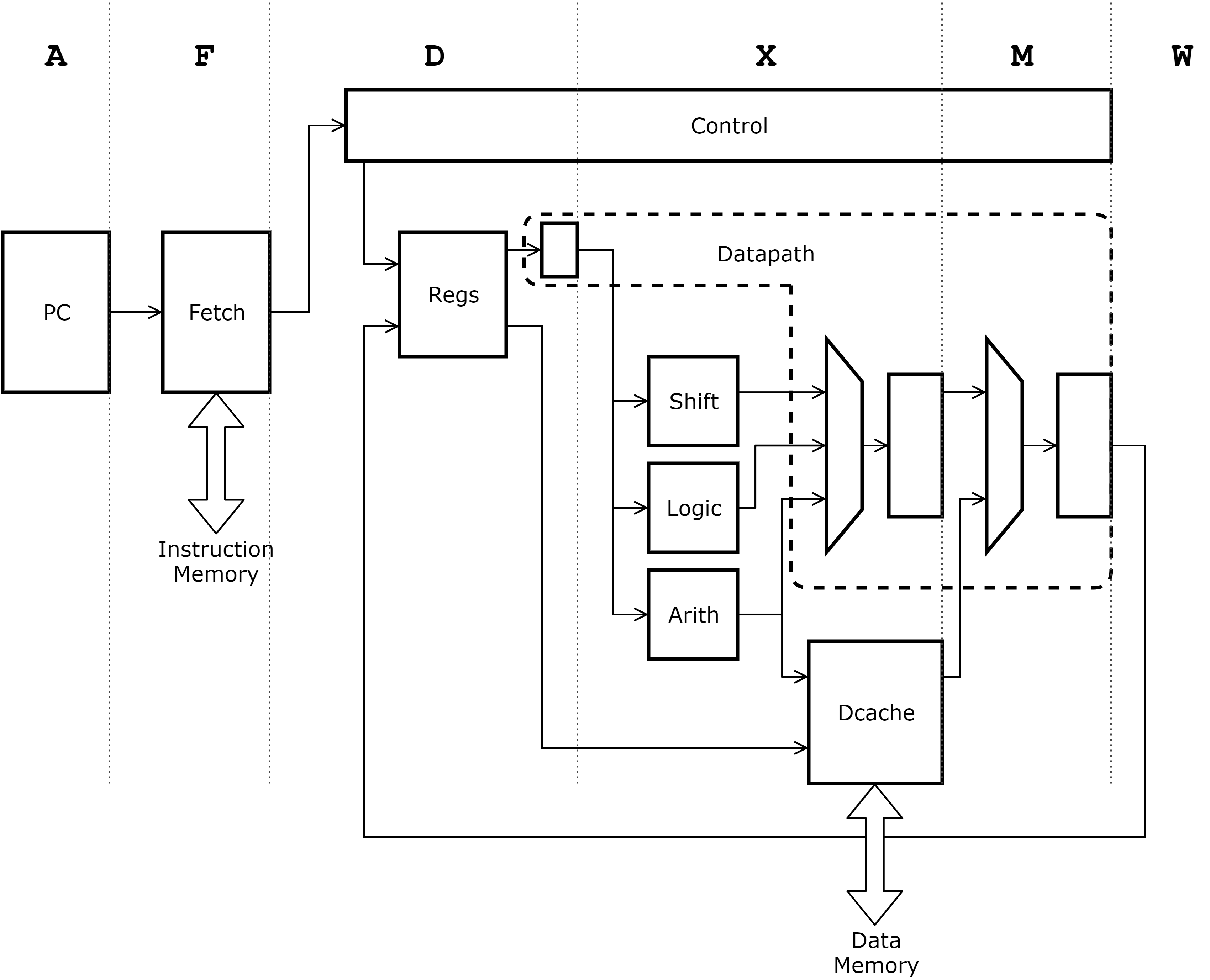
In the address stage we will make sure that the program counter is either incremented or loaded from somewhere else. At the end of this stage the program counter should have a stage instruction address. In the fetch stage, we will use this address to fetch the data stored at the particular address of the instruction memory. In real life this would usually take multiple clock cycles and we would need to use a prefetch and caching strategy. However, for this exercise, we will assume that the data from instruction memory can be retrieved within one clock cycle.
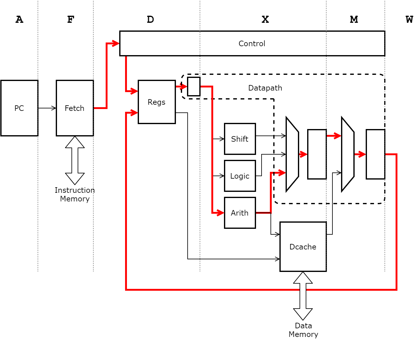
The fetch instruction will then be decoded in the control module which will select the proper signals to control the register file, the arithmetic block and other muxes in the datapath. The whole datapath for the add instruction is visualized here:
The register file is the module that holds the 64 registers of the processor. It will need dual read ports and at least one write port working at the same time to support the architecture we are designing.
Now that we know some of the basics, we can start coding. The first thing we are going to implement here is the program counter.
The proc_pkg package
We will keep all the constant values required by different modules of the processor in a single package proc_pkg. We will import this package from every module that need to use these constants. This package will need to contain all opcodes and other function values for distinguishing between the instructions. The implemented package that is good for this post can be found here.
Program Counter
The program counter is a register that holds the address of the next instruction that is going to be executed. In our case, the output of the program counter will go to the instruction fetch module which in turn will bring the instruction from the main memory. Since RV32 instructions are 32 bits each, the program counter needs to increment by 4 after starting to fetch a single instruction. Our program counter is going to need to load from multiple sources and increment the pointer when needed. We need to be able to load from so many sources to affiliate instructions like jump, return or to handle exceptions. However, for now we will just have the option to either increment the address by 4. We need to to reset the program counter to a known value. In our case we are going to reset to the address 32’h80000000. This is the same reset address used by rocket chip, and we are going to use the same address to be able to reuse the same linker scripts and make the code assembly easier.
Design wise our program counter is going to be very simple. It will have the typical reset, clock inputs as well as a control signal to tell it to increment by 4 when needed. For now it will have one output that is the current value of the program counter. The program counter register needs to either hold the current value or increment when the relevant signal is high. The counter logic should look something like this:
  always_ff @(posedge clk_i, negedge rst_n_i) begin
    if (rst_n_i == 1'b0) begin
      pc_q <= PC_RESET_VAL;
    end else begin
      pc_q <= next_pc;
    end
  end

  always_comb begin
    if (incr_pc_i == 1'b1) next_pc = pc_q + 'd4;
    else next_pc = pc_q;
  end
The complete program counter module up to this step can be found here
Fetch
The next step we will take is to design the fetch module. For now, this module will just pass the pc address to the instruction memory as instruction memory address and then load the output of the the instruction memory within one clock cycle. This is unrealistic in real life, where it usually takes multiple clock cycles to fetch the value from the memory. However, using caching techniques to pre-fetch data from the instruction memory can be utilized to make it seem like that the data is being fetched from the instruction memory within one clock cycle. For now, we will just assume that the data can be fetched from the instruction memory using the fetch module in just 1 clock cycle.
For this we will pass the program counter value directly as instruction memory address output. And for the output of the instruction memory which we will receive needs to be kept in a register. This register will be used as the output inst_o from this module.
The implemented fetch module can be found here
Regfile
The register file is the module that holds all 32 registers of the RISC-V processor. These include 31 actual registers and the zero register which always returns zero (and can not be written two). Since we do not need a physical register for the register zero, we will use an array of sized 31. The indexing of this array needs to start at 1 and end at 31. Since the address of the zero register is 0, this enables us to quickly decode the register address to the array index without using any kind of offset calculation. The array declaration will look like this:
logic [31:0] reg_content [31:1];We also need to read the registers with two different addresses simultaneously. We will use the read address values on the ports r1_addr_i and r2_addr_i to select the registers. The value of the selected registers using these address ports will be outputted on the ports d1out_o and d2out_o respectively. The read can happen in the same clock cycle the address is asserted. Hence the read logic can be in an always_comb block and the logic for both ports need to be independent. The logic is going to look like this:
  always_comb begin
    if (r1_addr_i == '0) begin
      d1out_o = '0;
    end else if (r1_addr_i == w_addr_i) begin
      d1out_o = din_i;
    end else begin
      d1out_o = reg_content[r1_addr_i];
    end

    if (r2_addr_i == '0) begin
      d2out_o = '0;
    end else if (r2_addr_i == w_addr_i) begin
      d2out_o = din_i;
    end else begin
      d2out_o = reg_content[r2_addr_i];
    end
  end
Similarly the register file can be written to using the ports w_addr_i and din_i ports. Since the address zero can not actually be written to, when the value of w_addr_i is set to 0, the writing will be effectively disabled. Hence, we can use the value 0 on the w_addr_i to keep the write port disabled as well when we are not using it. The writing logic needs to be in an always_ff block to make sure that the reg_content is treated as a “register”. It should look like this:
  always_ff@(posedge clk_i, negedge rst_n_i) begin
    if (rst_n_i != 1'b0) begin
      if (w_addr_i != '0) begin
        reg_content[w_addr_i] <= din_i;
      end
    end
  end
To be able to debug easily in simulation, we are going to add an initial block at the bottom of the regfile code. Without this the registers will be populated with random data at the start of the simulation. We will put some known “random” values instead to make our life easier. Here is the initial block that I will be using:
  initial begin
    reg_content[1] = 'd04;
    reg_content[2] = 'd27;
    reg_content[3] = 'd00;
    reg_content[4] = 'd83;
    reg_content[5] = 'd29;
    reg_content[6] = 'd58;
  end
Control
The control module will be responsible for decoding the instruction obtained from the fetch module. After decoding the instruction, the control module makes sure the proper control signals are sent to the proper modules at appropriate pipeline stage. In case of the R-Type instruction, the control module needs to read the appropriate register content from addresses rs1 and rs2 at the decode stage.
We will create registers which will hold the instruction opcode, the funct3, funct7, and rd. for each pipeline stage. We will discard instruction information that does not need to passed to the next stage and pass on the required information using to the appropriate register of the next stage.
For the decode stage we can use the registered instruction coming out of the fetch module directly. The value coming out of the fetch module needs to go through some logic (or directly) to generate the values for the execute stage registers. In our control module, we will have registers whose names start with x_ indicating these are registered values meant to be used in the execute stage. We will use similar prefixes for all subsequent stages as well.
For example, the d_opcode is just the bits 6 to 0 of the instruction coming out of the fetching module as input into the control module d_ints_i. This will be used to generate the x_opcode registered signal one clock cycle later. Similarly m_opcode is the same opcode value delayed by one more clock cycle and w_opcode is the opcode of that instruction at it’s writeback stage. We will eventually need to implement a mechanism for stalling the pipeline based on data conflict. However, for now we will assume no such thing and just implement the stages as if there is no conflict ever.
 always_ff @(posedge clk_i, negedge rst_n_i) begin
    if (rst_n_i == 1'b0) begin
      x_opcode <= '0;
      x_rd <= '0;
      m_opcode <= '0;
      m_rd <= '0;
      m_funct3_q <= '0;
      w_opcode <= '0;
      w_rd <= '0;
    end else begin
      x_opcode <= next_x_opcode;
      x_rd <= next_x_rd;
      m_opcode <= next_m_opcode;
      m_rd <= next_m_rd;
      m_funct3_q <= (x_opcode == LOAD_OPCODE) ? x_funct3_q : '0;
      w_opcode <= next_w_opcode;
      w_rd <= next_w_rd;
    end
  end

  always_ff @(posedge clk_i, negedge rst_n_i) begin
    if (rst_n_i == 1'b0) begin
      x_funct3_q <= '0;
      x_funct7_30_q <= '0;
    end else begin
      x_funct3_q <= x_funct3_next;
      x_funct7_30_q <= x_funct7_30_next;
    end
  end

  always_comb begin
    next_x_rd = d_rd;
    next_m_rd = x_rd;
    next_w_rd = m_rd;
    next_x_opcode = d_opcode;
    next_m_opcode = x_opcode;
    next_w_opcode = m_opcode;
  end

  always_comb begin
    d_rd = '0;
    x_funct3_next = '0;
    x_funct7_30_next = 1'b0;
    case (d_opcode)
      RTYPE_OPCODE: begin
        d_rd = d_inst_i[11:7];
        x_funct3_next = d_inst_i[14:12];
        x_funct7_30_next = d_inst_i[30];
      end
    endcase
  end
Datapath
The datapath module will redirect the data to and from the arith, logic, shift units as well as diverting it to and from the data memory unit and the register write back port based on the instruction that is in the appropriate pipeline stage. We will use the registered signals x_arith_op1 and x_arith_op2 as inputs to the arith block, m_alu_data as the registered signal that will capture either the output of the arith, the logic or the shift block and the registered signal w_mux to capture either the output of the data memory or the m_alu_data register. Since we are just going to implement the ADD instruction for now, there is going to be only one data path. We will hard wire this data path for now. The combinational logic for this is going to look like this:
  always_comb begin
    m_alu_data_next = arith_out_i;
  end

  always_comb begin
    x_arith_op1_next = reg1_data_i;
  end

  always_comb begin
    x_arith_op2_next = reg2_data_i;
  end

  always_comb begin
    w_mux_next = m_alu_data_q;
  end
The registered signals generated from these signals need to be inside corresponding always_ff block as well. This always_ff block once implemented will be as follows:
  always_ff @(posedge clk_i, negedge rst_n_i) begin
    if (rst_n_i == 1'b0) begin
      m_alu_data_q <= '0;
      x_arith_op1_q <= '0;
      x_arith_op2_q <= '0;
      w_mux_q <= '0;
  end else begin
      m_alu_data_q <= m_alu_data_next;
      x_arith_op1_q <= x_arith_op1_next;
      x_arith_op2_q <= x_arith_op2_next;
      w_mux_q <= w_mux_next;
    end
  end
The w_mux output needs to be connected to the register write port at the core level. Since we are always going to set the output of the arith block at the execute stage to the w_mux at the write back stage, and since the control module will set the appropriate register write address at this stage, this will enable us to write the appropriate value to the appropriate register at this pipeline stage.
Putting it All Together
At the core level we need to instantiate all of these newly implemented modules. We also have to make sure to declare all the local signals appropriately. Simulation using verilator will run without errors if local signals are not declared properly. However, these signals will only be single bit signals and might cause us huge debugging headaches if we don’t declare the signals properly now. We have the incr_pc signal floating since we have not implemented its driving logic in the control module yet. Let’s tie that signal to 1 using an assign statement in the core for now as well. The core.sv file at this stage can be found here.
Simulating our Instruction
To simulate our newly implemented instruction, we first need to write a hex file to populate our instruction memory with. For this testing we will use this simple program:
add x2 x0 x0
add x3 x1 x0
add x6 x5 x4
The first instruction will add x0 and x0 and put it in x1. Since the value of x0 is always 0 after executing this will put the value 0 into x1. The second instruction will add x2 with 0 and put it in x3. The third instruction will add x5 with x4 and put it in x6. We can take a look at the RISC-V ISP Spec (Table in Chapter “Instruction Set Listings”) to convert these into hex values. Once converted into hex it will be as follows:
00000133
000081B3
00428333
The code is written in hexadecimal. We need to pad the hex values with 0 such that each instruction takes up exactly 4 bytes. For convenience we can have instruction in a single line and make sure each instruction is 8 characters long.
We will need to save this as a hex file in vsim/hex/add.hex.
Before running the simulation, we need to make sure our Makefile is correct after adding a lot of new source sv files. If we look at line 59 of our Makefile, we had added -I../src there. So verilator should be able to pick up all files from the src directory. However, since we added a package in the proc_pkg.sv file and this package is imported from other source files, it needs to be always compiled before the other files importing it. So, we are going to change the Makefile line 59 to this:
VERILATOR_INPUT = tb/top.sv ../src/proc_pkg.sv -I../src -I./models -f input.vc sim_main.cppIn other words, we are making sure that the proc_pkg.sv file is compiled before other src sv files.
Now to run the simulation, we need to run this command from the vsim directory:
make HEX=hex/add.hexWe are explicitly setting the add.hex file path as the HEX variable.
If everything worked as it should, we will see the following message at the end of the run log in the terminal:
-- DONE --------------------
To see waveforms, open vlt_dump.vcd in a waveform viewer
Now we can view the waveform using gtkwave.
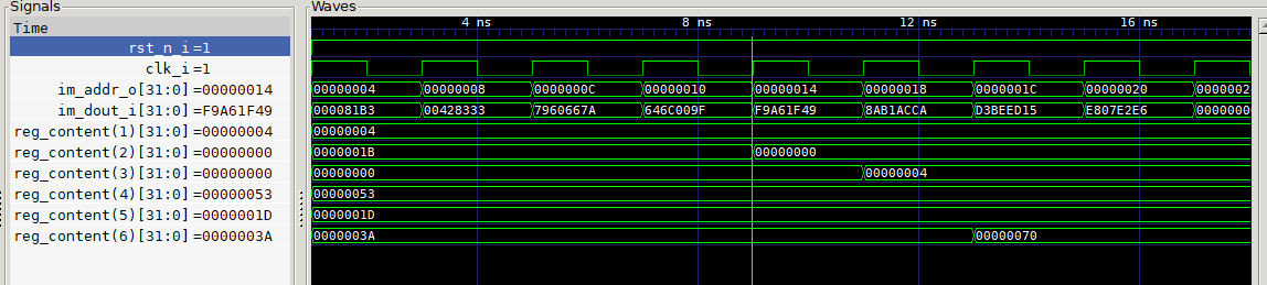
From the waveform we will need to plot the following signals: at the core level clk_i, im_addr_o and im_dout_i and reg_content(1 to 6) at the regfile level. We can see that im_addr_o signal starts at 0x0 at reset and increments by 0x04 every clock cycle after. This represent the value of the program counter and since our incr_pc signal is tied to 1 it increases every clock cycle. We can see that the im_dout_i changes with the change of the program counter value as well. If we look at the regfile content array, we will see that the values of the register changes based on our program. For example the first instruction was supposed to set x2 to 0. If we look at reg_content(2), it should be showing changing to 0x00 as expected around 9 ns. Similarly the next clock cycle we will see that the reg_content(3) changes to 0x04. The next clock cycle we see that reg_content(6) change to 0x53+0x1D = 0x70 as expected.
The processor RTL and simulation code up to this point can be found here
Pipeline conflict
One thing we have been avoiding in so far is pipeline conflict. Let’s assume that an instruction has the destination rd=x2. And the instruction immediately after that uses x2 as rs1. Now if the second instruction of these two start before the former reaches the writeback stage, then the second instruction will have the wrong value of x2. So we need to somehow stall the second instruction until the first instruction manages to finish it’s write back to the regfile.
The way we are going to do this is we are going to look at rs1 and rs2 and if it matches with the rd of any subsequent stage, then the core is going to indicate a conflict and stall the new instruction at the decode stage until the conflict is gone. For example, if we see the instruction add x1 x2 x2 at the decode stage, and if either x_rd, m_rd or w_rd holds x2, then we will know there is a conflict. This code can be done in a combinational block:
  always_comb begin
    if (reg1_addr != '0 &&
        (reg1_addr == x_rd || reg1_addr == m_rd || reg1_addr == w_rd))
      conflict = 1'b1;
    else if (reg2_addr != '0 &&
             (reg2_addr == x_rd || reg2_addr == m_rd || reg2_addr == w_rd))
      conflict = 1'b1;
    else
      conflict = 1'b0;
  end
We need to make sure we implement the instruction stalling logic, which needs to hold the current instruction present at the decode stage, as well as stall the program counter from going any forward. So we will use the output signals incr_pc_o and conflict_o which will go to the pc module and the fetch module respectively. We already have the logic for incr_pc in the program counter. The logic for holding the last instruction needs to be implemented in the fetch module. For this we are going to make sure that the inst_o signal works as before when conflict_i is 0 and it holds the previous value of inst_o when conflict_i is 1.
The new fetch module can be found here.
With these logic in place we need a simple testcase. We will use this program:
add x2 x0 x0
add x5 x2 x2
The first instruction will make x2 0. And then the second instruction should take the new value from x2 and put it into x5. If everything works properly, we should see both x2 and x5 registers becoming 0 after the execution of these two instructions. We are going to put the machine code in the file hex/add2.hex and it should look like as follows:
00000133
002102B3
We can run this program with our new processor code from the vsim directory using command:
make HEX=hex/add2.hex
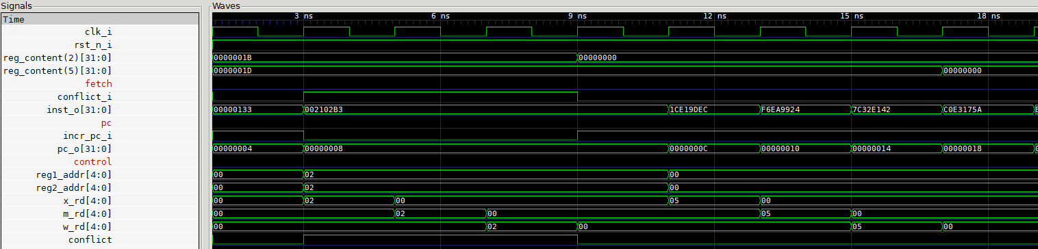
After the code execution is done, we can open the vcd waveform file from the logs directory using gtkwave. Let’s start by looking the the signals in the program counter. If we plot the signals incr_pc_i and pc_o, we can see that incr_pc_i goes down sometime and the value of the pc pc_o stops incrementing at that time. Next, we can take a look at the fetch module. If we plot the signals conflict_i and inst_o, we will see that the fetch module holds the value of the instruction while conflict_i is 1 and goes back to using pc to fetch next instruction once the conflict is over. We can also look at the signals reg_content(2) and reg_content(5) in the regfile module. Both of these registers should become 0x00 at the end of the execution of the two instructions as expected!
The entire processor core implementation up until this post can be found here.